
3D sensor chip and solution provider Adaps Photonics completed a C2 round funding
In the first half of 2024, Adaps Photonics experienced rapid business growth, entering the supply chains of several leading Chinese industrial companies. The company achieved mass production and shipment of high-end chip projects, significantly accelerating revenue growth beyond previous years. Against the backdrop of the company's rapid development and the opportunity presented by China's shift toward high-tech industries and the comprehensive development of intelligent ecosystems, Zhejiang Jinkong's Jintou Dingxin has completed a Series C2 investment in Adaps Photonics, focusing on core hard-tech investment. The funds from this round of financing will be continuously used for the rapid iteration and mass production of high-end 3D camera chips. By playing the role of a hardware enabler, the company aims to advance the technology of high-end 3D camera chips for smart driving, robotics, and high-end cameras, making "2D and 3D imaging integration, flexible and generalized end-to-end intelligent perception, and extreme low-light high-frame-rate imaging" a reality.
Adaps Photonics
Adaps Photonics, founded in May 2018 by several Ph.D. graduates from Stanford University and Delft University of Technology, has a core team with extensive experience in SPAD technology. The company boasts internationally leading full-stack SPAD device design and process capabilities and holds numerous domestic and international patents for self-developed SPAD technologies. It has been recognized by the Ministry of Industry and Information Technology as a national-level specialized and innovative "Little Giant" enterprise.
Adaps Photonics has launched products such as SiPM, single-photon imaging SPAD array chips, and multi-point and limited-point dToF chips and modules. It continues to accelerate the application of its products in areas such as smart cars, high-end mobile phones, robotics, automatic control, human-machine interaction, and smart home systems.
In 2021, the company successfully completed the wafer production of 3D stacked SPAD array chips. In 2023, it developed the world's highest pixel SPAD array chip, achieving solid-state 3D camera imaging.
The company achieved a world record in PDE parameters with its 905nm SiPM, reaching 25%, and obtained AEC-Q102 Grade 1 automotive-grade certification in 2023. The product performance meets the rigorous standards for automotive lidar in terms of performance and reliability, with stable and scaled mass production realized by the end of 2023.
Multi-point and limited-point products have continuously entered the supply chains of various leading manufacturers throughout the year, with ongoing product iteration and batch shipments.
The investment head of Jintou Dingxin commented, “Adaps Photonics is at the forefront of the high-end SPAD array chip process, being the only 3D sensing chip design company in China directly competing with international companies from Europe, the US, and Japan. The company views array and solid-state technologies as the inevitable direction for the evolution of lidar sensing chips and systems. With high-end 3D cameras as a business opportunity, Adaps Photonics is catching up with international giants in design and process capabilities, continually reducing SPAD pixel size and increasing pixel count. Coupled with modular development technology, the product not only continuously improves SPAD performance but also lowers costs. The ability to continuously reduce SPAD pixel size and increase SPAD integration is a core technical capability for 3D sensing chip companies.”
Adaps Photonics’s millions-of-pixels array chips are set to hit the market soon. The company's array imaging chips have a strong technological foundation, and its technology roadmap leads the progress of both domestic and international research and development communities. The ADS6311 chip released by ADAPS Photonics in August 2023 represents the most advanced large-size SPAD array product in the industry, with a photodetection area equipped with 768x576 SPADs, and each 3x3 SPAD forms a super pixel, achieving a 256x192 point cloud resolution. The ADS6311 is one of the market’s ultra-high-resolution pure solid-state lidar SPAD array chips, widely applicable in fields like automotive and robotics lidar, and has secured contracts with many leading technology companies both domestically and internationally.

ADS6311
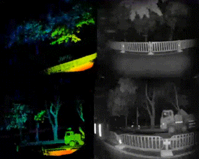
In-Car Animation 1: Roadside Barrier and Oncoming Lane
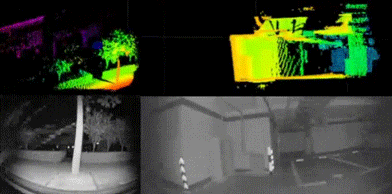
In-Car Animation 2: Bicycle Lane and Sidewalk, Underground Parking Garage
As a core component of pure solid-state 3D cameras, the development of SPAD array sensors has strategic significance in defining the performance limits of entire systems. Future 3D cameras will require only 3D stacked SPAD array chips, a transmitter, and a lens, evolving lidar from a “precision instrument with moving parts” to a “mass-producible 3D camera device,” significantly reducing costs for autonomous driving lidar. Meanwhile, as AGV, AMR, humanoid robots, and surveillance cameras move toward intelligent, networked, and interactive development, industry demands for sensors are increasing, and clients in industrial control and security fields are leaning towards automotive-grade products. Adaps Photonics’s automotive-grade certification and market validation lay a solid foundation for expanding into industrial control and security application scenarios.
Adaps Photonics has continually accumulated research and development capabilities for 3D sensing chips. Through multiple generations of product planning and ongoing iterations, the company has solidified its technological leading edge in high-pixel SPAD array products. Simultaneously, the company has efficiently combined technology and market needs, accelerating the scaled production of high-end intelligent scenario products. Step by step, Adaps Photonics will continue to lead market development as a leader in the high-end 3D SPAD array chip process, competing with international giants in the cutting-edge hard-tech and intelligent perception fields.
Copyright © Adaps Photonics All rights reserved  粤公网安备号44030502004595 粤ICP备19128428号-1